Journal Name: Journal of Pediatrics and Infants
Article Type:Research
Received date:30 December, 2019
Accepted date:16 March, 2020
Published date:16 March, 2020
Citation: Abasov FP (2020) Management Eletro Physical Properties Double-Barrier Structure Based on Silicon Radiation Defect. Int J Nano Rech Vol: 3, Issu: 1 (13-17).
Copyright: © 2020 Abasov FP. This is an open-access article distributed under the terms of the Creative Commons Attribution License, which permits unrestricted use, distribution, and reproduction in any medium, provided the original author and source are credited.
Abstract
Developed and analyzed double-barriers structures based silicon with high sensitivity integrated in the short range. The effect of gamma radiation on the mechanism of current transport in the structure type Schottky barrier, and in the p-n junctions. It is shown that the double-barrier structure can improve the photovoltaic parameters of conventional detectors. We studied the effect of gamma radiation on the origin of the current mechanism in the structure as a whole, and in the Schottky barrier in the p - n - transitions separately. Also studied the effect of radiation on the photoelectric and photoluminescence parameters of the two barrier structure. Shown that two barrier structures can improve the photoelectric parameters of conventional detectors. The photo detector on the basis of silicon with the increased integrated sensitivity in short-wave area of a range is developed. Influence radiation scale on the mechanism of a currents of both in structure like Schottky’s barrier, and in р - п - transitions is investigated. It is shown that two-barrier structures allow to improve photo-electric parameters of traditional detectors. Investigated the impact of radiation on the photoelectric and photoluminescence parameters of two-barrier structures.
Keywords:Silicon Photo Detectors, Two Barrier Structure, р - п –Transitions, Schottky Barrier, Photo Luminescence.
Introduction
Two barrier structures have been developed and analyzed - based on silicon photodetectors with high sensitivity shortwave spectrum. We studied the effect of gamma radiation on the origin of the existing mechanism in the structure as a whole, and in the Schottky barrier and p - n - transitions separately. Also, the effect of radiation on the photoelectric and photoluminescence parameters double-barrier structure has been studied. It is shown that the two barrier structures can greatly improve the characteristics of conventional photoelectric detectors. The effect of radiation on the photoelectric and photoluminescence parameters of the two barrier structures. Silicon photodetectors, still the most widespread type of photo converters.
One of the main directions of increase of speed and increase in spectral sensitivity of modern receivers of radiation with one transition is creation of multi barrier structures, in which thanks to internal strengthening and growth of coefficient of collecting of the photo generated carriers - it is possible to improve significantly key parameters which meet the requirements and needs of optoelectronics. Reliability of work of the received structures under the raised conditions of radiation, as detectors of ionizing radiation is an actual task and makes a subject of our researches.
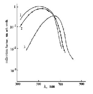
Recently for expansion of area of spectral sensitivity methods [1-4] bringing to photocurrent growth in shortwave area of a range are widely used. Example can is – Verizon band structures; pulling fields, etc., based on reduction of speed of a superficial recombination. In our case such opportunity, but in planar execution it is possible to create at the expense of a field n-p-transition included in the opposite direction. In the figure 1 dependence of the gathering of the wavelength of incident radiation double-barrier structure, p-n- junction and Schottky barrier.
Optical properties of films from the hν dependence (αhν)1/2 allows to determine the width of the band gap [5,6] for each film. In all the studied films of the coefficient of the optical absorption edge is described by the relation:
áhí = B(hí - E0)²
where, α=5∙104÷105 cm-1. E0 - optical band gap for each film. B - coefficient of proportionality. The value of B is determined by extrapolating depending on hν for each sample. The quadratic dependence (2) obtained theoretically for a model of Tauc [7], which describes the density of states of the mobility gap. The value of B at x = 0 ÷ 1 is from 527 to 343 eV-1, sm1/2, respectively, E0 = 1,14 ÷ 1,86 eV for films with Au-(p-n-)Si.
It is showing great interest in the study of photoluminescence features (PL) of short-wave radiation in the visible spectrum for efficiency c-Si-solar cells [8-11]. Thus, the problemimprove efficiency (c-Si) – photo elements consists of two parts: 1 - the re-emission of short-wavelength photons in the visible spectrum edge through the mechanism of direct optical transitions zone-zone silicon monohydrate, 2 - the effective conclusion of photogenerated carriers across the spectrum of solar radiation.
The forms of the spectra of these emissions, normalized to its maximum value each symmetrical with respect to the line:
where, vex - the frequency of the exciting radiation; vζ - frequency fluorescent light.
When excited photoluminescence monochromatic radiation is most likely the appearance of a low-frequency fluorescent light, although it is possible and the emergence of a high-frequency (anti-Stokes) radiation. The spectra of the Stokes and anti-Stokes photoluminescence emissions. Spectral rules of photoluminescence due to the fact that the absorption of the exciting photon with energy.
Wв = hvв ,
where, h - Planck constant;
vв - the frequency of the exciting radiation,
Wl = hvl ,
where, vl- fluorescent light frequency.
The energy difference Wb – Wl spent on various processes in the material, in addition to photoluminescence. In cases where a photon energy of the exciting radiation is added to some of the energy of the thermal motion of the phosphor particles
Hvl = hvb + akT,
where, a - coefficient depending on the nature of the phosphor;
k - is Boltzmann constant;
T - absolute temperature of the phosphor, there is antiStokes photoluminescence.
Technique of Experiment and Discussion of Results
Features of two-barrier structures created on one plane are for the first time received and studied. It is shown advantages before traditional structures. For creation of photodetectors of planar execution with internal strengthening Au-Si Schottky barrier is created. As an initial material the structure р - n - type on a silicon substrate is used.
The realization of management by current by means of light was enabled by selection of supply voltage of K-E in such a way that collector transition is closed, and emitter — is open, at free base. Under the influence of light in it electrons and holes are generated. At collector transition there is a division electronic hole couples which have reached owing diffusions of border transition. Holes are thrown by a field of transition to a collector, increasing own current, and electrons remain in base, lowering its potential.
Thus on emitter transition there is additional direct tension that strengthens injection of holes from the emitter in base. The injected holes, reaching collector transition cause additional increase in current of a collector. As total collector current is proportional to coefficient of internal strengthening, increase of spectral sensitivity - reaching 0,65A/W.
The purpose of work consists in studying of influence of a charging condition of no equilibrium vacancies on processes occurring during radiation and silicon heat treatment with Nn =1016 sm³, and also clarification of the mechanism of increase in integrated sensitivity of two-barrier structures of rather ordinary photo diodes.
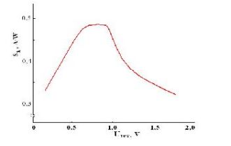
In figure 2 spectral characteristics of two-barrier structure before radiation are shown, at the room temperature at the return tension of Ucont. = 0B, and Ucont. = 0,5B. From drawing it is visible that with growth of the enclosed return shift on r-p-transition photocurrent increases what to lead to photosensitivity growth, at an optimum choice of the return tension on r-p-structure transition.
At further increase in Ucont spectral sensitivity falls. Such behavior of Sλ connected with growth of area of a volume charge and improvement of coefficient of collecting of photocarriers. With a further growth of Ucont because of overlapping of zones, photoinjection of BSh is blocked and the structure works in a mode of one photo diode figure 3.
The structure was irradiated at T=300 K in gamma quanta of Co60. Isochronous (30 min.) annealing of radiation defects was carried out in the range of temperatures of Ta = 200-450 K.
Method of photo MF of
I showed that primary radiation defects (RD) in p-Si crystals at 300 K are loaded positively.
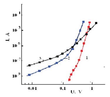
The analysis VAC figure 3 and spectral characteristics showed that recombination currents increase in process of increase in a dose of radiation. Annealing of diodes leads to decrease in recombination currents [12]. At Ta temperature ≈ 300°C there is an annealing and reorganization of divakansion to formation of the V2 complexes + O, and at Ta = 350°C the A-centers (V + O) and complexes (V2 + O) are actively annealed. The analysis of change of a current of through BSh and n-p- transition showed distinction of influence of annealing near a surface and in the depth of a crystal. It can be explained with growth of a photo response of BSh connected with accumulation of a charge and improvement of coefficient of collecting.
In figure4 shows the dependence of spectral sensitivity and photo clip of the structure on the reverse mixing of p-njunction.
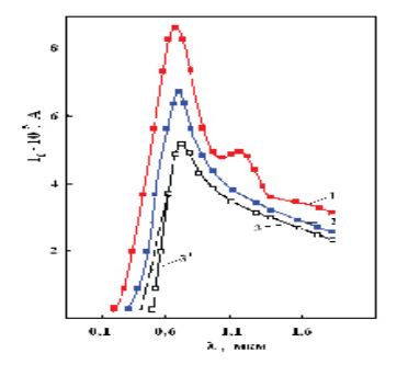
In figure 5 curves of spectral dependence of photocurrent before and after radiation scale are represented at various doses and after annealing at T=400°C within 30 min. Annealing influences spectral characteristics slightly. With dose increase the radiation scale growth of photocurrent decreases.
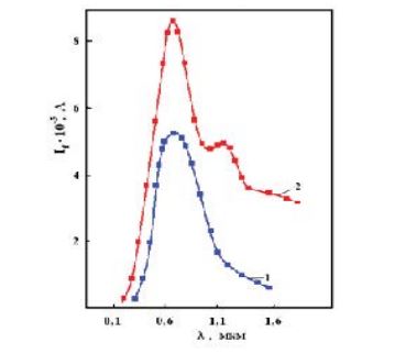
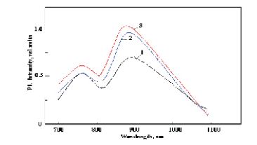
In figure 6 photo luminescence spectra of samples irradiated with gamma rays spectral rules of photoluminescence due to the fact that the absorption of the exciting photon with energy.
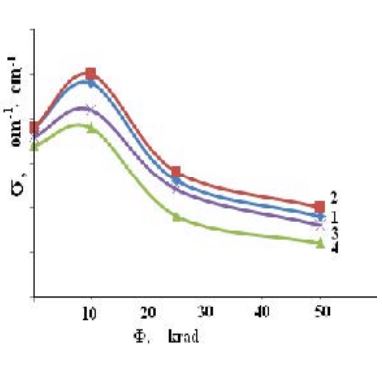
In figure 7,8 relaxation of photo conductivity when excited it rectangular pulse.
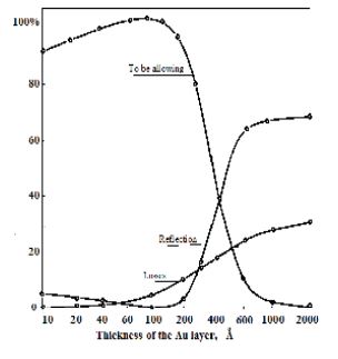
Figure 1: The dependence of reflection, absorption and conductivity of the metal (Au) thickness in the structure.
Figure 2: The dependence of the gathering of the wavelength of incident radiation:1. double-barrier structure2.Schottky barrier3.p-n- junction
Figure 3: Spectral characteristic of the double-barrier structures to radiation 1.-Urev.=0V2.-Urev.=0.5 V. T = 300 K
Figure 4: Dependence of the spectral sensitivity of the structure the applied reverse bias the p-n-junction.
Figure 5: Volt-ampere characteristics of p-n-junction.1.original.2. Dγ = 10 kGy.3. Dγ = 20 kGy. Annealing results are in sign.
Figure 6: Spectral characteristic double-barrier structure after irradiationwithgammarays:1-up irradiation, 2-dose 1,5 kGy, 3) dose of 2,0 kGy.,3’) annealed at T= 400°C for 30min.
Figure 7: PL spectra of samples irradiated with gamma rays: 1- prior to irradiation, 2-Dγ – 1,5 kGy., 3) Dγ – 2,0 kGy.
Figure 8: Relaxation of photoconductivity when excited itrectangular pulse. 1-U=0,3 V, 2-U=0,5V, 3-U=1,0V, 4-U=1,2V.
Conclusion
Thus, it is possible to claim that the main role in electric losses the studied silicon structures is played by the oxygencontaining centers (V2 +O and V + O). At increase in a dose of radiation and increase in temperature of annealing, feature VAC and spectral characteristics are caused by change of resistance of n-Si (basic area of structure), the caused accumulation (at increase in a dose) or disappearance and reorganization (when annealing) radiation defects. It is known that the speed of capture by defect of electrons and (or) holes first of all depends on the section of capture and the provision of power level in the forbidden zone. These parameters in fact are the “individual” characteristic of defect [5,6].
When annealing structures there is a reorganization of dot radiation defects and their disappearance. Thus mainly there is an accumulation of the same defects. Comparison to literary data shows that the main role in photo-electric losses of the studied structures is played by the oxygencontaining centers (V2+O and V+O). At further increase in a dose of radiation there is an irreversible reduction of photosensitivity due to significant increase in resistance of base.
Sze SM (1984) Physics of Semiconductor Devices, New York: Wiley[ Ref ]
Bakaleynikov LA, Flegontova EJ, Pogrebitsky K, Eremin IV (2004) Theoretical principles of semiconductor detector based on the p-n junction. Technical Physics 49: 1181-1190.[ Ref ]
Savchenko IV (1985) Theoretical Foundations of dosimetry.[ Ref ]
Kosyachenko LA, Maslyanchuk EL, Rarenko IM, Sklyarchuk VM (2004) Research carrier collection CdZnTe ray detectors and-radiation photoelectrically. Semiconductors 38: 981-986.[ Ref ]
Abasov FP (2016) Study of radiation effects on photoelectric and luminescence parameters of two-barrier structures based on silicon. 2nd International Conference on Condensed Matter physics which is going to be held on October 26-28, in Chicago, USA.[ Ref ]
Abasov FP (2016) Determining the amount of hydrogen in thin films well for solar cells. International Journal of Scientific Research in Engineering 1: 01-14.[ Ref ]
Madatov RS, Mehrabova MA, Abasov FP (2006) Fast acting detectors for - quantums on the Au-Si. The IV euroasian conference on nuclear science and its application. Baku, Azerbaijan.[ Ref ]
Madatov RS, Abasov FP, Mustafayev Yu M (2011) Effect of gamma radiation on photovoltaic parameters of a two-barrier structure based on silicon. Russian Conference on Semiconductors Novosibirsk 22-26.[ Ref ]
Abasov FP (2014) Getting thin films to create solar cells /”PHOTO” 2: 72-90.[ Ref ]
Abasov FP (2014) Influence of gamma radiation on electrik propertien of silicon solar cells. Internatiolnal journal of Pure and Aplied Science and Technology 21: 12-16.[ Ref ]
Abasov FP (2014) Effect of gamma irradiation on electrophysical and photoelectric parameters of double-barrier structure based on silicon. Nuclear Science and its Application Vll Eurasian Conference. Baku, Azerbaijan.[ Ref ]
.Abasov FP (2016) Effect of Gamma Irradiation on Photoelectric Parameters of Double-Barrier Structure Based on Silicon. Journal of Material Sciences and Enginering USA 5: 269. [ Ref ]
